
 Intro
Intro
Thats me, Dhrubajyoti Samanta a.k.a. DJ. Sorry for this late intro. Just couldn,t think of anything to write. I had joined the summer camp at Calcutta with all the others. I had also played football with others. So long for now. Waiting for your comments.
Monday, January 22, 2007
Friday, January 19, 2007
CALL FOR HELP
Arun , or ne1 else, plz get me a DATASHEET for the Transistors TL - 188
and TL - 187 ... EMERGENCY !
Sorry for posting this but I really need this ASAP !
TWISH
( Soon get bak with a REAL Post )
Friday, January 12, 2007
HaPpY BiRtHdAy Mr. TiMe!!
Happy Birthday Saurya (Time) Mishra!! H*A*P*P*Y* .* .*.* .* .* .* .*.* .* B*I*R*H*D*A*Y
Hope you enjoy Your Day!
Time flies doesn't it?? Better come up with time travel soon....
*.* .* .* .* .* .() ().() () () () () .* .* .*.* .*
.* .* .* .*.* .* || || || || || || || .* .* .*.* .*
.* .* .* .* . *@@@@@@@@@@ .* .* .*.* .*
.* .* .* .* .*@/////////////////////////@ .* .* .*.* .*
.* .* .* . *@@@@@@@@@@@@@@@@ .* .* .*.*
.* .* .* .* @//////////////////////////@ .* .* .*.*
.* .* .* @@@@@@@@@@@@@@@@@ .* .* .*
.* .* .* @///////////////////////////@ .* .* .*
.* .* .* @@@@@@@@@@@@@@@@@ .* .* .*
.* .* .*.* .* .* .* .*.* .* .* .* .*.* .* .* .* .*.* .* .* .*
:D
Monday, January 08, 2007
Basics of Electronics: Transistor Time!
Woo! Transistors! Drool, drool. Ok, my childish reactions apart, transistors are the backbone of electronics as we know it. They represent a control structure, where you can control one part of the circuit with another (as a master-slave relationship). As an overview, a transistor has 3 terminals (I'm talking about BiJunction Transistors' (BJT) here), which are called the Emitter, Base, and Collector (EBC). By changing the potential difference between the Base and Emitter, the current between the Emitter and Collector can be varied. I'm going to use acronyms for EBC's from now on, because I'm lazy.
Generic NPN transistor diagram below:
Ok, we'll discuss the NPN (negative-positive-negative) transistor right now. The PNP transistor is nearly the same, except the polarities are reversed. So the NPN transistor consists of three regions, a N junction (see previous article for junctions), a P junction and a N junction. They are the Collector, Base and Emitter respectively. If you want to, you can look at the transistor as two diodes, with the P junction fused. You can take two PN diodes and try to make a transistor out of it, but it'd be really crappy, because the P junction must be very very thin for reasons we shall soon see.
Let's connect up our transistor to a battery, and try and understand how it works:
Firstly, note that the C is connected in reverse bias (i.e. the positive end is connected to it), with respect to the EC connection. The BE is in forward bias though. Remember the depletion zone (from the previous article) right? Well, its here too. By varying the potential difference between the BE, we are able to change the 'thickness' of the depletion layer. That allows more current to flow. Initially, the layer is pretty thick, and electrons can't flow from the E to the C, so there is no current in the EC circuit. Now, as we increase the potential between BE, the layer thins down. So now electrons are allowed to flow into the B region.
Remember that the EC in reverse bias? That means that the C can't give electrons because of the gap, but it does mean that it is very very eager to take electrons. Thus, it sucks up the electrons that enter the B region. The B region must be very thin so that the electrons are not absorbed by the B or taken away from the circuit.
There you have it folks, by varying the BE potential, you vary the depletion layer. This allows a current into the B region, which is taken up again by the C region (so the Collector collects the current). Through a model, the relation between the V(BE) and I(EC) is Ice is proportional to exp(Vbe) (exp is e power). There are other components called FET (field emmission transistors), which vary as Ice proportional to Vbe^2.
In the next article, we'll discuss Op-amps, Comparators and Logic Gates
(Did I catch yous in time for the PBs?)
Sunday, January 07, 2007
Basics of Electronics: Diodes
Well, this is going to be a lengthy specialized article. I don't know how many of you have worked with circuits (as in solder circuits), but I atleast can vouch for myself, and Twish. I'll just explain what goes on behind the diode, the transistor, and the op-amp. We've already covered the others, i.e., resistors, capacitors and inductors in our syllabus (technically, diodes are in my syllabus too, but we've not covered them). I'll then go on to explain a very very simple IC, the 555 timer. I'm not sure at this point whether do post them as parts or as a whole. But I resolved to finish the entire article today, so at least I can post the bits and pieces over a few days.
Diode:
First, lets look at the generic diagram of a simple P-N junction diode:

The 'P' junction is a semiconductor (generally silicon) doped with a trivalent element, like boron, so that it becomes an electron-deficient species. They have electron acceptors, or 'holes'. As always, the guys behind this liked to complicate their lives and ours, so by convention, we talk of the 'holes' moving, rather than electrons. The trivalent dopant atom (Boron), cannot properly bond with the neighboring Si atoms; one of the four bonds lacks an electron, which it readily will accept from any source it can lay its hands on.
The 'N' junction is a semiconductor doped with a pentavalent element, like Arsenic, so that it has an extra electron (as compared to the usual four). They give out electrons. The As atom has an electron, after using four of its electrons to bond with its neighbors. The bond energy of this electron is pretty weak, and the electron can easily be cajoled into leaving.
Let's move on to the function of this simple device. As soon as you join these two 'junctions', the electrons from the N junction immediately 'neutralize' the holes of the P junction. This creates a void space in the middle in which there are no charge carriers. Note that a conductor conducts only due to carriers, and hence the absence of them makes the void space an insulator (a very thin one though). This region is called a depletion zone.
Now, as with all insulators, and all materials in fact, if you force it enough, you can get electrons to flow. When the holes and electrons have met, they leave behind a positive dopant ion, and a negative dopant ion. Yup, you know where I'm going with this, a field is established in the reverse direction. So, if you establish a sufficient potential difference between the two ends, the electrons have enough energy to make it through this gap, and current can be established. In general, I've seen most references say that the gap closes, but I feel that is simply a convention established, to easily explain the phenomenon.
A good question to ask at this point is after the electrons jump the gap, shouldn't they fall into the holes again? In fact, they do, and that is why there is some potential drop across diodes. A key difference between semiconductors and conductors is the number of electrons/holes it has is finite. That means that you can fill them all, and go on with life. That is why the graph of the I-V of a diode isn't just a right angled line.
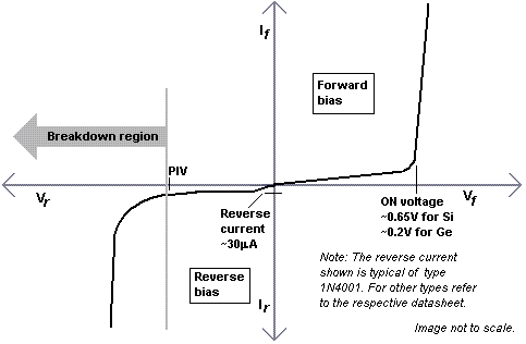
There are two ways a diode can be connected, forward bias and reverse bias.
Forward Bias: In this setup, the positive (or higher potential end) is connected to the P junction, and the negative (or lower potential end) is connected to the N junction. This will establish from P -> N. That means the electrons are pushed from N -> P, which is a good end. The N junction has excess of electrons anyway, and the depletion layer potential is in the P -> N direction. So the external field overrides the internal field, and the electrons merrily cross the depletion layer. Once the potential of the depletion layer is reached, the current jumps up to its normal value, from a meager trickle earlier.
Reverse Bias: If you were to flip the connections, and connect the P junction to the negative terminal, and vice versa, then you would create a field in the direction of the internal field, increasing the gap. You would get no current in this manner. However, if you increase the potential enough, the material of the diode breaks down, and suddenly allows a lot of current to flow. This is called avalanche breakdown.
Now you know how a diode works. I know most of you already know this stuff, but I had to clear the way for the other topics.
Coming Soon: Transistors...
Friday, January 05, 2007
Biology & Astronomy - Questions, not Answers
Alright. Two things being tossed off my mind here.
1) Why February?
So when the calender was first made (gregorian), the months were given days according to the motion of the moon. Also, it was noted that a year is about 365.25 days, so a leap year was added every four years to negligate the approximation of 365.
However, it was noted that the days in one month had to be truncated to fit in 365. And then they truncated them from Feb. And now we can't rely on the day of the month to find the location of the moon.
But why were these days removed only from Feb? Why weren't the number of days in every month made equal?
2) Negative Half-Life?
Although a half life is negative, as in it is for decomposition, is there anything opposite to the phenomenon of exponential decomposition?
Take the example of Cancer cells. They divide, then the two cells again divide etc. The rate of reproduction increases over time. My question is, is there an accurate exponential formula for this? There really should be, according to physics, but there may be factors which inhibit the reproduction of a particular daughter cell of a cancereous parent...
3) Time travel
You will just have to wait for the release of my book.![]()
Thursday, January 04, 2007
Introducing...
Hello, people.
I am not one of the "bright students of India getting the KVPY Scholarship". Nope. I'm just here for the absurdity of it all.
So let me introduce myself. I am Rohit Garg. Also called RG.
First off, I'm sort of obsessed with light and invisibility (and spinvisibility). Also studying the possibilities of time travel.
I also like blood as a colloid buffer. I am partially insane, but I believe you geniuses (or genii) can put up with that.
Also love computers.
Subscribe to:
Posts (Atom)

