
Basics of Electronics: Diodes
Well, this is going to be a lengthy specialized article. I don't know how many of you have worked with circuits (as in solder circuits), but I atleast can vouch for myself, and Twish. I'll just explain what goes on behind the diode, the transistor, and the op-amp. We've already covered the others, i.e., resistors, capacitors and inductors in our syllabus (technically, diodes are in my syllabus too, but we've not covered them). I'll then go on to explain a very very simple IC, the 555 timer. I'm not sure at this point whether do post them as parts or as a whole. But I resolved to finish the entire article today, so at least I can post the bits and pieces over a few days.
Diode:
First, lets look at the generic diagram of a simple P-N junction diode:

The 'P' junction is a semiconductor (generally silicon) doped with a trivalent element, like boron, so that it becomes an electron-deficient species. They have electron acceptors, or 'holes'. As always, the guys behind this liked to complicate their lives and ours, so by convention, we talk of the 'holes' moving, rather than electrons. The trivalent dopant atom (Boron), cannot properly bond with the neighboring Si atoms; one of the four bonds lacks an electron, which it readily will accept from any source it can lay its hands on.
The 'N' junction is a semiconductor doped with a pentavalent element, like Arsenic, so that it has an extra electron (as compared to the usual four). They give out electrons. The As atom has an electron, after using four of its electrons to bond with its neighbors. The bond energy of this electron is pretty weak, and the electron can easily be cajoled into leaving.
Let's move on to the function of this simple device. As soon as you join these two 'junctions', the electrons from the N junction immediately 'neutralize' the holes of the P junction. This creates a void space in the middle in which there are no charge carriers. Note that a conductor conducts only due to carriers, and hence the absence of them makes the void space an insulator (a very thin one though). This region is called a depletion zone.
Now, as with all insulators, and all materials in fact, if you force it enough, you can get electrons to flow. When the holes and electrons have met, they leave behind a positive dopant ion, and a negative dopant ion. Yup, you know where I'm going with this, a field is established in the reverse direction. So, if you establish a sufficient potential difference between the two ends, the electrons have enough energy to make it through this gap, and current can be established. In general, I've seen most references say that the gap closes, but I feel that is simply a convention established, to easily explain the phenomenon.
A good question to ask at this point is after the electrons jump the gap, shouldn't they fall into the holes again? In fact, they do, and that is why there is some potential drop across diodes. A key difference between semiconductors and conductors is the number of electrons/holes it has is finite. That means that you can fill them all, and go on with life. That is why the graph of the I-V of a diode isn't just a right angled line.
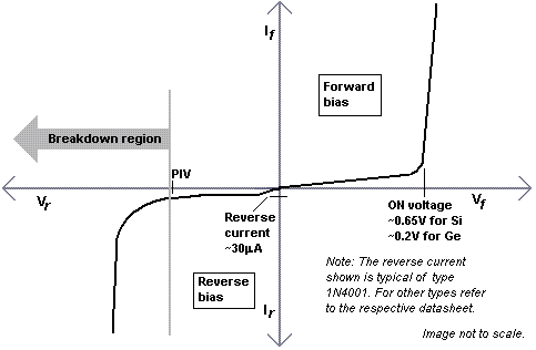
There are two ways a diode can be connected, forward bias and reverse bias.
Forward Bias: In this setup, the positive (or higher potential end) is connected to the P junction, and the negative (or lower potential end) is connected to the N junction. This will establish from P -> N. That means the electrons are pushed from N -> P, which is a good end. The N junction has excess of electrons anyway, and the depletion layer potential is in the P -> N direction. So the external field overrides the internal field, and the electrons merrily cross the depletion layer. Once the potential of the depletion layer is reached, the current jumps up to its normal value, from a meager trickle earlier.
Reverse Bias: If you were to flip the connections, and connect the P junction to the negative terminal, and vice versa, then you would create a field in the direction of the internal field, increasing the gap. You would get no current in this manner. However, if you increase the potential enough, the material of the diode breaks down, and suddenly allows a lot of current to flow. This is called avalanche breakdown.
Now you know how a diode works. I know most of you already know this stuff, but I had to clear the way for the other topics.
Coming Soon: Transistors...


4 comments:
Twish n I used to solder together
under the "supervision" of Mr.Dhingra, which was really super. Except that there was no vision involved.
Humm it reminds me that I better revise Semiconductors for my preboards or else I'll fail in it too, as I would in todays paper - Maths :(
PS: I always wanted to take up Electronics and Robotics, but just got stuck up with Maths Lab :D Still I'll surely take them up when I go to a college (that is only when I get into one having such facilities :D)
And yeah, Transistor ke bare mein post jaldi karna... isi bahane semiconductors revise ho jayega!
:D
when's your transistor exam? I'll post it right now (in an hour I'll have typed it up. I lied about having finished it already)
Post a Comment